AMD's "Venice": Pioneering the Future of Computing with TSMC's 2nm Technology in Taiwan
AMD's Next-Gen EPYC Processor "Venice" Leads the Charge with TSMC's Cutting-Edge 2nm Node, Ushering in a New Era of High-Performance Computing.
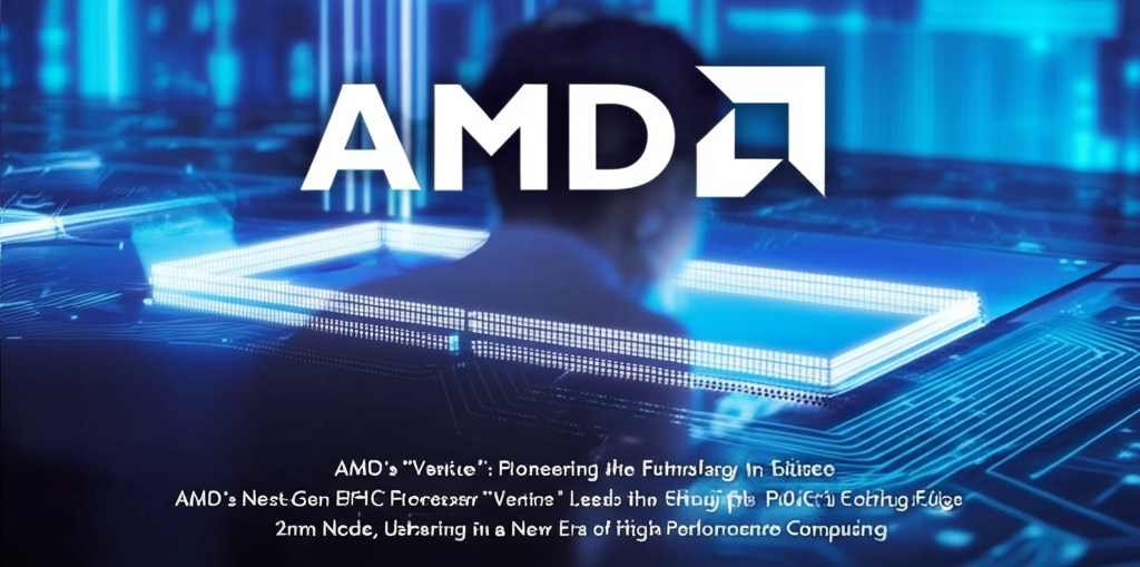
Taipei, Taiwan – April 15 - Advanced Micro Devices, Inc. (AMD) has announced that its next-generation EPYC processor, codenamed "Venice," will be the first high-performance computing (HPC) processor to utilize Taiwan Semiconductor Manufacturing Co.'s (TSMC) groundbreaking 2-nanometer (2nm) process. This marks a significant leap forward in the realm of advanced computing, solidifying the strong partnership between AMD and TSMC and placing Taiwan at the forefront of semiconductor innovation.
In a statement released Tuesday, AMD confirmed that the "Venice" processor has successfully completed the "tape-out process," the final stage of integrated circuit design before mass production. The launch of this innovative processor is slated for next year, promising to revolutionize data center capabilities and performance.
This achievement is a direct result of the collaborative efforts between AMD and TSMC. According to AMD, the two companies co-optimized new design architectures with cutting-edge process technology through their longstanding partnership. The collaboration aims to maximize performance and efficiency in the upcoming "Venice" processor.
AMD CEO Lisa Su (蘇姿丰) recently visited TSMC Chairman and CEO C.C. Wei (魏哲家) at TSMC's headquarters in Hsinchu. This visit underscored the close relationship between the two companies and coincided with TSMC's planned commencement of 2nm process production in the second half of this year.
The new HPC processor "Venice" is also a major step forward for AMD's data center CPU roadmap, highlighting the company's commitment to delivering innovative solutions to meet the ever-growing demands of the computing industry. Further emphasizing its commitment to US manufacturing, AMD also highlighted the successful validation of its 5th Gen AMD EPYC central processing unit (CPU) products at TSMC's new wafer fab located in Arizona.
"TSMC has been a key partner for many years and our deep collaboration with their R&D and manufacturing teams has enabled AMD to consistently deliver leadership products that push the limits of high-performance computing," stated AMD's Lisa Su.
Lisa Su further added: "Being a lead HPC customer for TSMC's N2 process and for TSMC Arizona Fab 21 are great examples of how we are working closely together to drive innovation and deliver the advanced technologies that will power the future of computing."
Fab 21, the first TSMC fab in Arizona, began mass production in 2024 using the 4nm process.
In response, TSMC's Wei (魏哲家) expressed pride in the partnership, stating, "By working together, we are driving significant technology scaling resulting in better performance, power efficiency and yields for high-performance silicon."
TSMC is currently constructing a second fab in Arizona, with commercial production anticipated in 2028, utilizing the 2nm and 3nm processes. The company is also planning to initiate construction on a third fab in the state, with the 2nm or more advanced processes expected to be used.
Sponsor